A 4 MG Static S-100 RAM Board
Most S-100 users
have a few RAM boards in their system. Early systems often consisted of 4K,
8K or 16K boards. With the advent of 16K dynamic RAM chips in the early 80's
64K dynamic RAM boards became common. The most popular being the SD Systems
ExpandoRAM series. When 16 bit CPU boards appeared most vendors
utilized static RAM chips because of their easier interface requirements.
64K and 256K S-100 static RAM boards were popular and were very reliable.
For example the
BG Computer 256K RAM card was typical. By the mid 80's a few 1MB and 2MG static RAM boards were made by
CompuPro
and Macrotech. However these were expensive and few were actually made.
Today the scene is very different. Gigabyte dynamic RAM chips are common
place and 512K X 8 bit static RAM chips are commonly available. (Higher
capacity static RAM chips are also available but as far as I know not in DIP
configurations).
Since I intend to build up my S-100 System to accommodate fast and memory
hungry CPUs like an 80386 etc. I decide to build a high capacity RAM board.
Eight 512X8, thirty two pin DIP chips should easily fit on an S-100 board
and yield a capacity of 4MG. Four such boards will fully stock the
S-100 bus with 16 MG of RAM. There are a few versions of such RAMs out
there. I opted for the Alliance Memory
AS6C4008 32 pin
DIP chips. These are available from Jameco (part # 1927617). Just two
chips will give you 1MG of RAM -- enough for any 8086/80286/DOS
requirement!
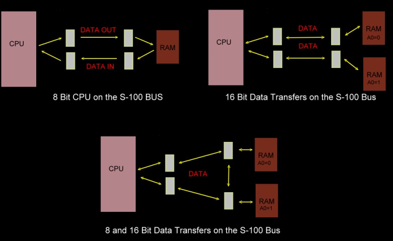
Memory Board Logic The S-100 bus was designed around the 8080 CPU. This CPU has a
bi-directional 8 bit data path, however because Ed Roberts wanted to control
it via a series of front panel switches, the CPU data bus was broken out
into separate 8 bit Data In and Data Out paths on the S-100 bus.
This worked fine. RAM boards had their RAM chips connected to both data
paths and I/O boards were likewise connected. It was a somewhat
inefficient setup but it worked (all for a simpler front panel).
The first diagram below shows the basic layout.
When 16 bit CPU's came along things got more complicated. All 16 bit
CPU's have a 16 bit bi-directional data path. They can interface
directly to RAM chips that are 16 bits wide or two 8 bit wide RAM chips. In
the early 80's the latter type of RAM's were much more common. Two 8 bit
wide RAM chips differing only in address line A0 (0 or 1), would be
connected to the 16 bit bus. The S-100 Data In and Data out lines were
utilized together as a single bi-directional 16 bit bus and were connected
via buffers to the CPUs 16 data line pins.
Now if all you were going to use was such a 16 bit CPU that would be fine.
But such a setup would not work with older 8 bit RAM cards or indeed with
any I/O cards which also expect a split 8 bit interface.
The solution was simple and elegant and the heart of the IEEE-696 standard.
For 16 bit systems the bus behaves as a 16 bit bidirectional bus. For 8 bit
systems a bridge buffer on each RAM board transfers the data coming and
going to the board over separate 8 bit data lines depending on whether it's
address is odd or even. If we have 8 bit data coming to the board on an even
address, it travels on the "Data Out" path and goes directly to the A=0 RAM
bank. If instead the 8 bit data is destined for an odd address it
arrives as before at the RAM board top buffer but then is dropped down to
the lower A0=1 RAM bank via a bridging buffer.
If the 8 bit CPU wants to read a even address it activates this buffer in
the opposite direction so the RAM A=0 bank data is shifted down to the S-100
data in lines. If the 8 bit CPU wishes to read am odd RAM address the A0=1
RAM bank data travels directly to the CPU on the Data Out bus.
The hardware logic to do this is quite tricky. You need to factor in if we
have a CPU read or write, if the data is 8 bits or 16 bits wide and if the
destination address is on an even or odd address line. (Fortunately no
common 16 bit CPU transfers 16 bit data an odd address line).
Now back in the mid 80's companies like CompuPro and Macrotech implemented
this logic in ROM like chips called PAL's. Unfortunately they never
published the code.
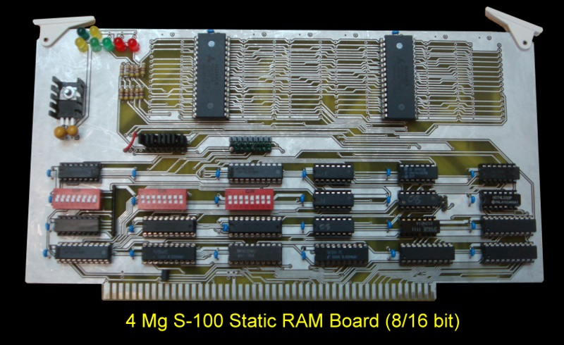
A First Prototype 4 MG Static RAM Board
I wanted to build a S-100 RAM board that would serve me well into the
future. Where I could use it with very fast and wide CPU's. I decided
against Dynamic RAM because of the complexity of refreshing (particularly
for Master/Slave CPU switching). Likewise I wanted to stick with DIP type
chips. There are higher density RAM chips than 512K/chips we use here but
they require SMT and are difficult to work with. The 32 Pin DIP
Alliance AS6C4008 seemed like the way to go, (Jameco Part #1927617).
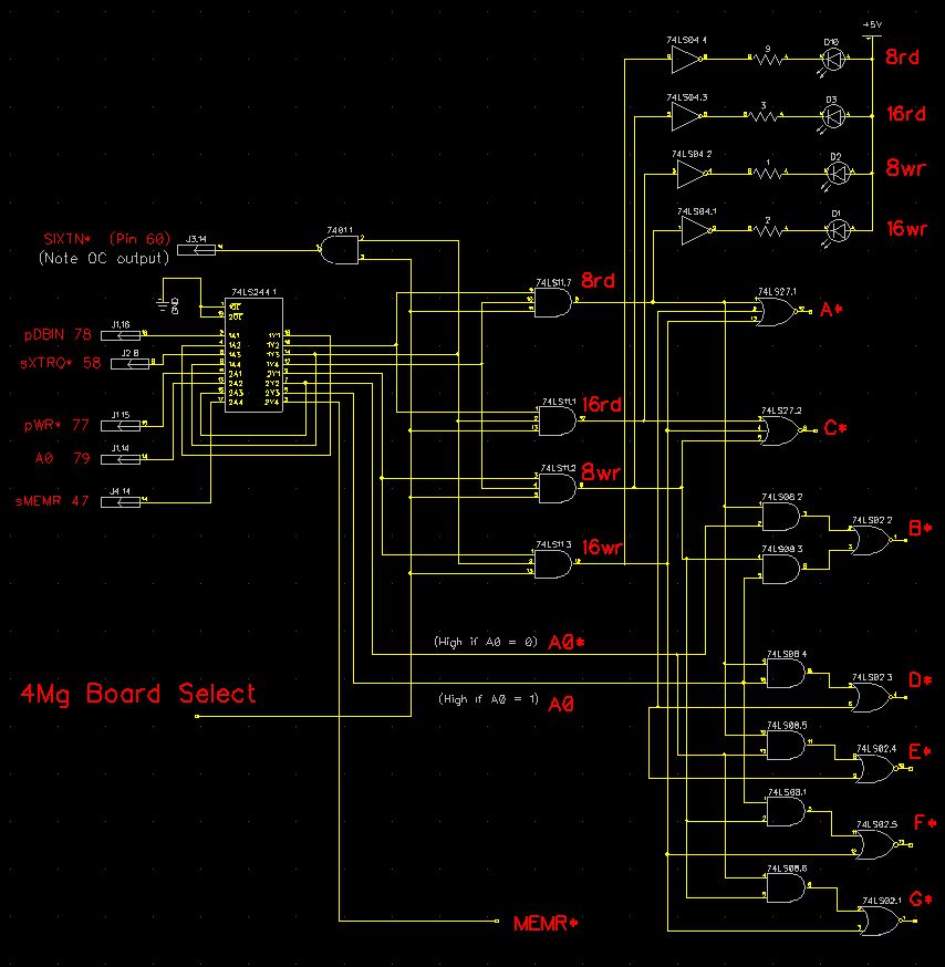
The hardest part was figuring out a PAL equivalent circuit using standard
TTL chips. I came up with the following "7400" TTL layout. It takes a few chips as opposed
to one PAL but it is fast and reliable.
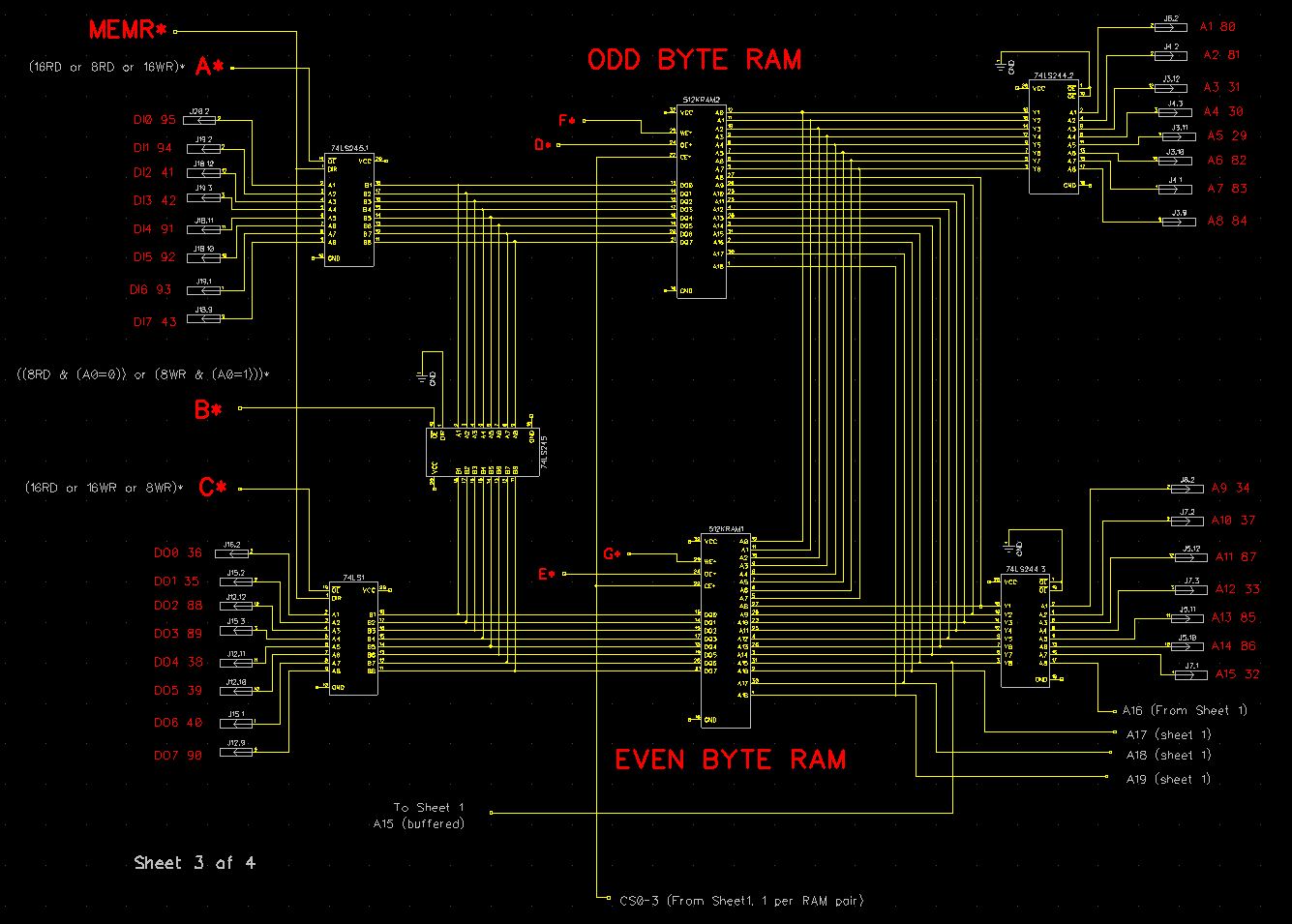
The above logic interfaces to the high and low RAM banks as follows:-
Since this was a completely untested design with Andrew Lynch at N8VEM (see
here) we made a
"pre-production" prototype board. The schematic of
this board can be seen
here.
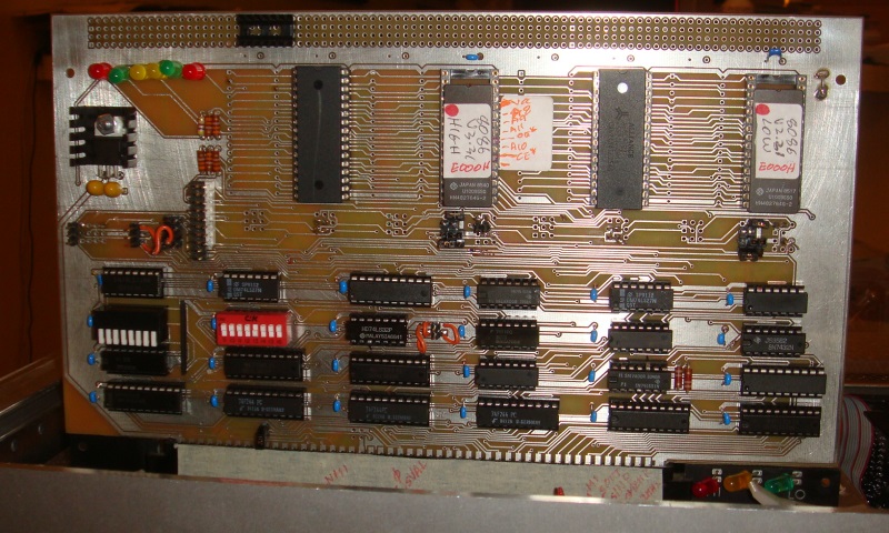
You will notice that the board accommodates both static RAM chips, Flash RAM
chips and EPROMS (from 2716's all the way up to 27256's). Here
is a picture of the board.
You will notice a "patch area" above the normal height of an S-100 board for
further prototyping/repairs etc. Fortunately we did not need to add any
chips.
The board works solid as a rock with an Intersystem's 4MHz Z80 CPU board
(including its ability to address above 64K) and with my own IEEE-696
compatible S-100 8086 and 80286 boards -- later write-ups! I have not
determined the maximum speed of the board yet but considering the chips are
rated at 55ns, I expect the bus itself would be the limitation.
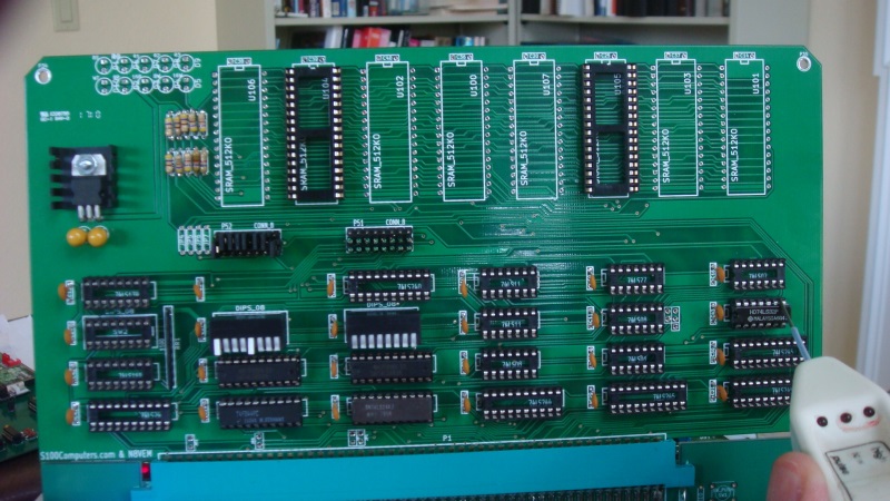
4 MG Static RAM Board Prototype-II With lessons learned from this board we made a second RAM only
prototype board using the following
schematic and
diagram. We will do a separate EPROM/Flash board later. This is a
somewhat simpler board since now there is no need for all the configuration
jumpers for the many types of possible EPROM's. Here is a picture of
this prototype RAM board:-
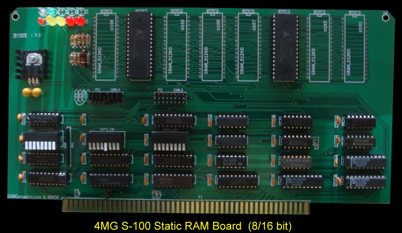
The Final 4 MG Static RAM S-100 Board
The above board had worked without any problems for four months in two
systems using CPM+ and CPM86 with verity of hardware configurations so
Andrew and I decided to go ahead and do a final commercial type board.
The trace layout was optimized further before doing this. Here is a
picture of the final 4 MG S-100 Static RAM board.
Building The 4 MG Static RAM S-100 Board
While at first the circuitry may seem complex it is really fairly simple.
There are four components. The circuitry consists of:-
Select RAM board addressing
Carry out 8/16 bit data transfers
Wait state circuitry (if needed)
The RAM chips themselves.
The above board works fine in all systems I have. This includes CPM+ and a
750K version of CPM86+. With 59 ns access times on the RAM chips
clearly no wait states are currently needed. I have the circuitry there for
a later 80385/80486 CPU board I will be doing.
Realizing that a number of others have
expressed an interest in obtaining these bare boards and building a board
themselves . I have below a step by step procedure as to help build the board.
While the board is simple to build and debug, its clearly not for a "first
timer". Very little hand holding can be provided, sorry this is not a
commercial operation!
The trick in assembling S-100 boards like this is to assemble it in
functional sections. Sure you can put everything together in one large
bite and take a chance, but I have long since found in the end, a systematic
step by step approach is faster.
First check add the board 5 volt regulator and two capacitors. There is an
error on the silk screen on the board and in the schematic above. Both C1
and C3 should be 33uF capacitors (not .33 and .1uF). If you use
tantalum caps, make sure the polarity is correct. All capacitors
should be 10 volts at least but C1 should be at least 25V. Plug it into an
S-100 extender card and check you have exactly 5 volts at each 5volt pin for
each chip position.
Next add all sockets, filter capacitors and 470 ohm resistors (R1-R10).
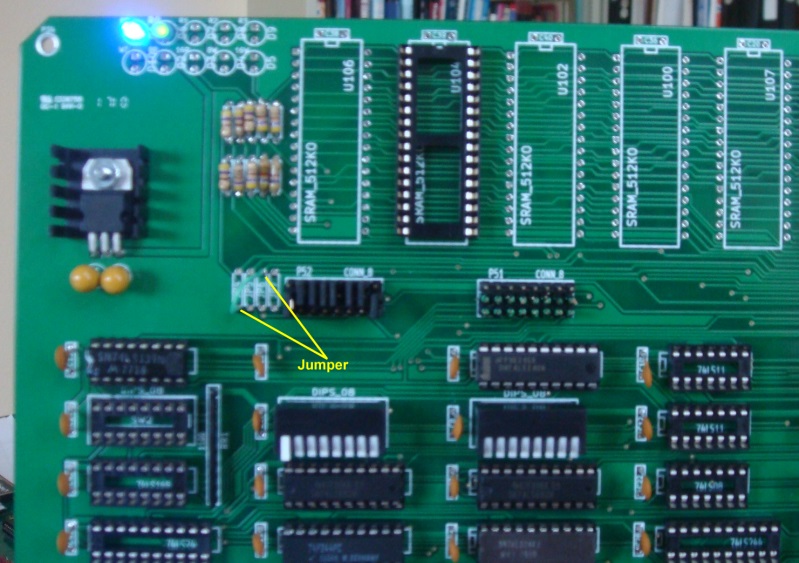
Insert the rows of jumpers for address selection (P49-P54).
Repeat the above voltage check.
Next we will add the board address selection circuitry. This circuitry
brings down the "4MG_RAM_Select" line when the correct RAM area (within the
S-100 16 MG RAM address space) is selected. With 4 MG/board, clearly just 4
such boards would fill all our S-100 needs. However in many cases
initial systems will be just Z80's (64K) or 8086 (1MG) RAM. So only one
board is required and only a pair or RAM chips at that. This is what we will
use here.
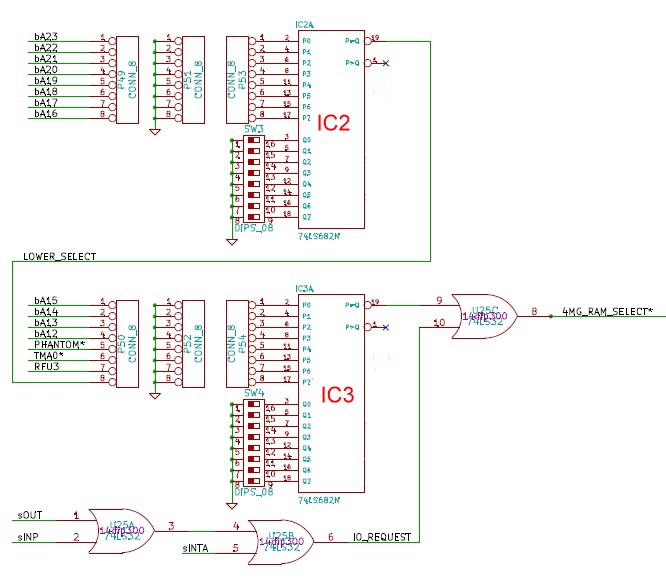
Here is a section of the Board RAM select circuitry:-
The board utilizes 74LS682's for RAM addressing. If your are unfamiliar with
this technique click
here.
The important point to remember is that both 74LS682's each have two sets of
inputs (P0-P7 & Q0-Q7). The chips compare each P input against each Q input
if all the Highs & Lows match up only then does pin 19 goes low. IC2(a) is for
RAM in the first 64K. If connector P49 pins are jumpered to P53 pins and all
SW3's are closed (to ground), ONLY when address lines A16 to A23 are zero
will IC2 pin 19 go low. The first 64K of RAM. If we connect
P50,#8 (bottom row), to P54,#8 (middle row) and SW4,#8 (rightmost switch) is closed/on
(ground) then we restrict the board to only the first 64K of RAM.
It's nice to be able to debug/bring up a board like this (with no RAM initially)
with another board in the bus so we can us a ROM based monitor
to debug the hardware. So let's restrict the board further to a 32K - 64K RAM
window.
Put an old 8K RAM board at address 0000H (for a stack for your monitor
software) in your system. Jumper P50,#1 to P54,#1 and set SW4,#1 (leftmost
switch) open/off
(high). Then only when Address line A15 is high will the board be active
(7FFFH-FFFFH).
So go ahead and add IC2 & IC3 (74LS682's), U2 & U24 (74LS244's) and U25
(74LS32) to the board. Insert it in your S-100
box and display memory. Now the Z80 refreshes S-100 RAM all the time so if
you just look at pin 8 of U25 it will always be pulsing low. The
question is when in a bus cycle. If we put code in our memory board at
0H such as:-
C3 00, 00
and jump to the location. The Z80 will be in a tight loop jumping all the
time to zero. Under these circumstances pin 8 of U25 will show high with
most logic probes. There is still a low going refresh pulse but it is now a
small percentage of bus time. Hit reset and it will go back to pulsing
low again.
This test assumes your ROM monitor is on your Z80 board and can overlap with
a RAM board in the 32-64K window. If your ROM is on another board you
may need to utilize the S-100 phantom line on our the RAM board. In this
case jumper P50, # 5 to P54, #5 and open SW4 #4 (high) so pin 12 of U3 is
high.
If you setup the jumpers as described above, pin #8
of U25 should go low only when RAM from 7FFFH-FFFFH is being displayed.
BTW make sure your monitor is not using low memory to store flags etc. Only
when you get the above correct go further.
Here is a picture of me checking out this step.
The above scheme is quite flexible. By adjusting A15-A12 you can create RAM
"holes" down to a 4K resolution. Useful for any ROM boards you may have
in your system.
BTW, the SOUT, sINP, sINTA circuitry is there to make sure the board is not
addressed for I/O operations -- particularly for interrupt acknowledge
situations.
Next we add in the following circuitry.
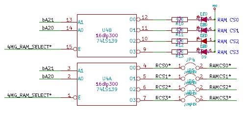
The 74LS139 (U4) looks at address lines A20 and A21 to determine where
within the boards bus 4MG address space each RAM chip pair will reside. There are
just 4 options. At 000000H, 010000H, 020000H and 030000H. Unless you
are using an 80286 or greater only the first option is used since a Z80 or
8086 is capable of only reaching up to 1MG of RAM. We will be using
more RAM with later CPU's in the future but for now one board is way more than enough!
Note; the remaining two S-100 Address lines (A22 & A23) are examined by IC2
and with 4 of these boards would determine where each (4MG board) would
reside within the 16MG address space, (in 4MG blocks), of the S-100 Bus.
They would reside at 000000H (this case), 040000H, 080000H or 0C0000H.
See the diagram and
schematic. Remember RAM chips are use in pairs
here. It does not matter which pair of slots you use for your 1st MG
of RAM its just RCSO* has to be jumpered to it (RAMCS0*, RAMCS1*, RAMCS2* or
RAMCS3*). I happened to use the RAMCS1* ((U104 & U105) pair. Also add
the chip RAM pair select LED's. Also add the 4MG Board select LED
(blue in my case). Here is a picture of the board at this stage.
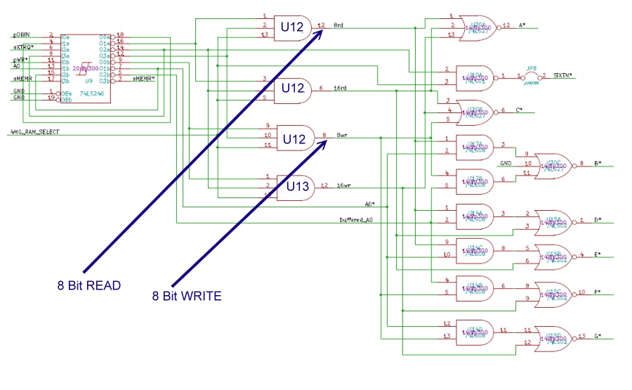
Next we add the rather complex circuitry that processes the data transfers
to/from RAM 8/16 bits wide. If you like, you can regard it as a black box.
Again step things along. See this circuit.
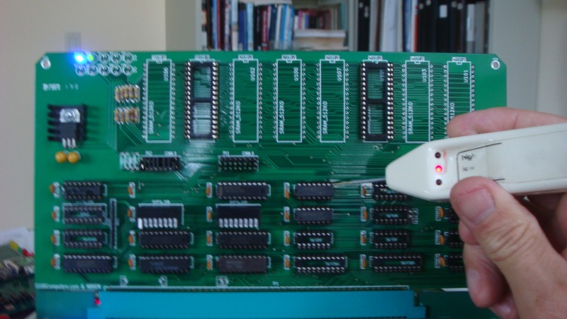
Insert just U9, U12 and U13. Do an 8 bit (Z80) memory read and write to RAM
at 0H and check you get a low to high pulse for a read or write as shown
above. Here is a picture of the process.
For now don't bother about 16 bit read/writes for now. Carefully add the
rest of the RAM read/write circuitry. Everything in the above schematic
which can be see better
here.
As I said above, the circuit has the ability to add 0-8 wait states to any
RAM read/write (See below). However since that circuit is not yet
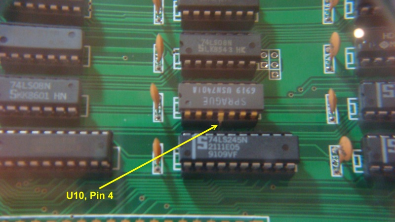
added, we need to (temporally) bend out pin #4 of U10 otherwise it will put
the bus in a hold state. Here is a
picture.
Repeat the above RAM read and write tests. Only go forward when
you are convinced the 8 bit Read and Write signals are correct. You can add
the remaining LED's which (if inserted correctly) will save you using a
logic probe. A common problem is people insert the LED incorrectly. First
just place the LED in the holes. Giggle it around. It should light up. If
not reverse the polarity. Only then solder it in place. You will not
damage the LED (assuming you have the 470 ohms resistors in place). In
order to have the write LED light up (very narrow pulses) fill memory from
8000H to A000H with 0's with your monitor and watch. I have found that the
smaller LED's really don't light up well with this narrow pulse. I use the
larger (red) LED's. I also used a 100 ohm resister instead of the usual 470
ohm to get more light.
Next we are ready for the critical test, the RAM test. Double check that
you are getting (only) 5 volts on pin 32 for the chip. These particular
RAM chips normally operate at 3.3 volts. They work fine at 5 volts, but 5.5
volts is the maximum. Carefully insert a RAM pair. Take the usual
precautions about static electricity. Also install the RAM buffers. Indeed,
everything on the board except U27 and SW2.
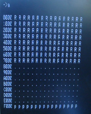
Check out the board. You should now see RAM at 8000H - 9FFFH with your monitor.
Check it out by changing and moving bytes etc with your monitor. You
can test the IC3 circuitry is working correctly by playing around with the
jumpers (1-3) of P50 and SW4. Here
is a RAM map (after I removed my 8K of RAM (see above) at 0000H) and
jumpered p50,#1 to P54,#1 and set SW4,#1 to ground (i.e. the board is only
active if A15 is low).
If you see this you are almost there. You can remove any other RAM board
from your system. You then can open the board up to its full 1MG
addressing capability by essentially cutting out the input from IC3A. We do
this by jumpering all the pins of P52 to P54 and setting all SW4 switches to
ground. This way U3 pin 19 is always low. The board is addressed
directly by the RAM chips (and A20 & A21 of U4).
There are some subtle inputs/things you can do with some of the connections
on P50 but this is for later boards and CPU's I will discuss them at that
time. For now ignore them. However if your system utilizes the Phantom
line for your ROM board/monitor jumper P50,#5 to P54,#5 and open SW4,#5.
So far we have just tested the board with 8 bit read and writes. For 16 bit
systems you will need a 16 bit CPU. I have tested the board on my own
IEEE-696 compatible 8086 & 80286 boards and ran it fine with CPM86+.
The circuitry is very clean and fast. It should work with most boards but of
course no guarantee. I have run it with a number of Z80 systems,
Intersystem's, Compupro etc. Absolutely rock solid -- in fact way overkill
for these CPUs!
The remaining circuitry is U27, the resistor pack RR1 and switch SW2.
You can bend in pin #4 of U10 at this stage also. This circuitry allows you
to add 0-8 wait states to any board read or write cycle. With 50ns RAM
chips --- clearly not needed by most current systems. However since I intend
to use this board in the future with very fast CPU's may as well have it
now. With all SW2 switches to the OFF position, no wait states will be
added the bottom left LED should never come on. Thanks to Kipp Yeakel
here is a parts
list for the board.
A Production S-100 Board.
Realizing that a number of people might want to utilize a board like this
together
with Andrew Lynch at N8VEM (see
here) we have
completed a run of these boards. We will collect names for a second
batch if needed. If
you have an interest in such a bare board, let Andrew know via e-mail at:-
lynchaj@yahoo.com Please note all the above
clearly applies only to people who know what they are doing and can do
a little soldering and board assembly. There will be little hand holding
at this stage.
Pontus Oldberg has recently sreported that switching to a 74F11 for U12 &
U13 and a 74F02 for U15 that this allowed him to use the board with a 68K
CPU at 10MHz.
See
here.
The links below will contain the most recent schematic of this board.
Note, it may change over time and some IC part or pin numbers may not correlate
exactly with the text in the article above. MOST
CURRENT 4MG STATIC BOARD SCHEMATIC
(V10, FINAL, 4/21/2010) MOST
CURRENT 4MG STATIC BOARD LAYOUT (V10, FINAL,
4/21/2010)
Other pages describing my S-100
hardware and software. Please click
here
to continue...